


Wild_C
@wild-c.bsky.social
Mostly AMD, Intel, and NVIDIA stuff
No sources or exclusive info
No sources or exclusive info
Is GB10 the high-end NVIDIA Laptop SoC?
Because otherwise why would it have an asymmetric CPU layout?
Looks like 2 clusters with 5x Cortex-X + 5x Cortex-A each
It also seems to have all the I/O you'd want for a Laptop
"1000 FP4 TOPS" (24TPCs?) would correspond GB205 (5070Ti Laptop) performance
Because otherwise why would it have an asymmetric CPU layout?
Looks like 2 clusters with 5x Cortex-X + 5x Cortex-A each
It also seems to have all the I/O you'd want for a Laptop
"1000 FP4 TOPS" (24TPCs?) would correspond GB205 (5070Ti Laptop) performance
January 7, 2025 at 4:33 AM
Is GB10 the high-end NVIDIA Laptop SoC?
Because otherwise why would it have an asymmetric CPU layout?
Looks like 2 clusters with 5x Cortex-X + 5x Cortex-A each
It also seems to have all the I/O you'd want for a Laptop
"1000 FP4 TOPS" (24TPCs?) would correspond GB205 (5070Ti Laptop) performance
Because otherwise why would it have an asymmetric CPU layout?
Looks like 2 clusters with 5x Cortex-X + 5x Cortex-A each
It also seems to have all the I/O you'd want for a Laptop
"1000 FP4 TOPS" (24TPCs?) would correspond GB205 (5070Ti Laptop) performance
I know this is just 1 benchmark, but... did Arm and MediaTek just take the mobile GPU crown?
Because that was not on my bingo card
Sauce:
youtu.be/__9sJsKHBmI
Because that was not on my bingo card
Sauce:
youtu.be/__9sJsKHBmI

November 23, 2024 at 1:23 PM
I know this is just 1 benchmark, but... did Arm and MediaTek just take the mobile GPU crown?
Because that was not on my bingo card
Sauce:
youtu.be/__9sJsKHBmI
Because that was not on my bingo card
Sauce:
youtu.be/__9sJsKHBmI
The Snapdragon X naming scheme almost looks like it was designed to be long enough so people wouldn't pay attention to it, which is very scummy considering the major differences between SKUs with the same branding
No way they need 6 digits + a letter to name these things
/1
No way they need 6 digits + a letter to name these things
/1

November 23, 2024 at 1:22 PM
The Snapdragon X naming scheme almost looks like it was designed to be long enough so people wouldn't pay attention to it, which is very scummy considering the major differences between SKUs with the same branding
No way they need 6 digits + a letter to name these things
/1
No way they need 6 digits + a letter to name these things
/1
Note to self:
Check that the math makes sense before posting it on the internet
No Ryzen processor announced or launched has >50TOPS of "AI performance"
And RDNA3 doesn't increase performance on INT8 over RDNA2, even though it is for FP32 and "AI" FP16/BF16
Check that the math makes sense before posting it on the internet
No Ryzen processor announced or launched has >50TOPS of "AI performance"
And RDNA3 doesn't increase performance on INT8 over RDNA2, even though it is for FP32 and "AI" FP16/BF16

November 23, 2024 at 1:21 PM
Note to self:
Check that the math makes sense before posting it on the internet
No Ryzen processor announced or launched has >50TOPS of "AI performance"
And RDNA3 doesn't increase performance on INT8 over RDNA2, even though it is for FP32 and "AI" FP16/BF16
Check that the math makes sense before posting it on the internet
No Ryzen processor announced or launched has >50TOPS of "AI performance"
And RDNA3 doesn't increase performance on INT8 over RDNA2, even though it is for FP32 and "AI" FP16/BF16
By the way, the official abbreviation for AMD Hawk Point seems to be "HWK", not "HPT"

November 23, 2024 at 1:21 PM
By the way, the official abbreviation for AMD Hawk Point seems to be "HWK", not "HPT"
A bunch of stuff seems to have been deleted from 🤔
This includes:
-10th/11th/12th Gen Core
-13th Gen Core i9
-Core i3 N-series
-"Intel Processor"
-3rd Gen Xeon Scalable
Even if you use search, a lot of SKUs (mostly DT) seem to be gone
ark.intel.com
This includes:
-10th/11th/12th Gen Core
-13th Gen Core i9
-Core i3 N-series
-"Intel Processor"
-3rd Gen Xeon Scalable
Even if you use search, a lot of SKUs (mostly DT) seem to be gone
ark.intel.com

November 23, 2024 at 1:21 PM
A bunch of stuff seems to have been deleted from 🤔
This includes:
-10th/11th/12th Gen Core
-13th Gen Core i9
-Core i3 N-series
-"Intel Processor"
-3rd Gen Xeon Scalable
Even if you use search, a lot of SKUs (mostly DT) seem to be gone
ark.intel.com
This includes:
-10th/11th/12th Gen Core
-13th Gen Core i9
-Core i3 N-series
-"Intel Processor"
-3rd Gen Xeon Scalable
Even if you use search, a lot of SKUs (mostly DT) seem to be gone
ark.intel.com
Die Size Measurements for Granite Rapids-AP UCC (left) and Sierra Forest-SP HCC (right):
-Birch Stream IO Die (shared): 241mm²
-GNR 44P UCC Compute Die: 598mm²
-SRF 144E HCC Compute Die: ~578mm² (large margin of error due to low res)
-Birch Stream IO Die (shared): 241mm²
-GNR 44P UCC Compute Die: 598mm²
-SRF 144E HCC Compute Die: ~578mm² (large margin of error due to low res)

November 23, 2024 at 1:20 PM
Die Size Measurements for Granite Rapids-AP UCC (left) and Sierra Forest-SP HCC (right):
-Birch Stream IO Die (shared): 241mm²
-GNR 44P UCC Compute Die: 598mm²
-SRF 144E HCC Compute Die: ~578mm² (large margin of error due to low res)
-Birch Stream IO Die (shared): 241mm²
-GNR 44P UCC Compute Die: 598mm²
-SRF 144E HCC Compute Die: ~578mm² (large margin of error due to low res)
It seems like we finally have some amount of consensus as to what Battlemage's specs will be
Putting all of the recent info together, BMG-G10's specs are:
-Xe² HPG architecture
-56 Xe Cores
-448 XVEs (EUs)
-2x shaders per XVE (like PVC)
-112MB Adamantine(?) Cache
-256-bit G6X bus
Putting all of the recent info together, BMG-G10's specs are:
-Xe² HPG architecture
-56 Xe Cores
-448 XVEs (EUs)
-2x shaders per XVE (like PVC)
-112MB Adamantine(?) Cache
-256-bit G6X bus

November 23, 2024 at 1:20 PM
It seems like we finally have some amount of consensus as to what Battlemage's specs will be
Putting all of the recent info together, BMG-G10's specs are:
-Xe² HPG architecture
-56 Xe Cores
-448 XVEs (EUs)
-2x shaders per XVE (like PVC)
-112MB Adamantine(?) Cache
-256-bit G6X bus
Putting all of the recent info together, BMG-G10's specs are:
-Xe² HPG architecture
-56 Xe Cores
-448 XVEs (EUs)
-2x shaders per XVE (like PVC)
-112MB Adamantine(?) Cache
-256-bit G6X bus
So apparently AMD is doing some rebranding of Xilinx's Alveo lineup
"Xilinx Alveo SN1022" is being rebranded to "AMD Alveo U45N", probably to better align with the lower end "Xilinx Alveo U25N"
SN1022 and U45N have the same specs:
xilinx.com/products/board… xilinx.com/products/board…
"Xilinx Alveo SN1022" is being rebranded to "AMD Alveo U45N", probably to better align with the lower end "Xilinx Alveo U25N"
SN1022 and U45N have the same specs:
xilinx.com/products/board… xilinx.com/products/board…

November 23, 2024 at 1:20 PM
So apparently AMD is doing some rebranding of Xilinx's Alveo lineup
"Xilinx Alveo SN1022" is being rebranded to "AMD Alveo U45N", probably to better align with the lower end "Xilinx Alveo U25N"
SN1022 and U45N have the same specs:
xilinx.com/products/board… xilinx.com/products/board…
"Xilinx Alveo SN1022" is being rebranded to "AMD Alveo U45N", probably to better align with the lower end "Xilinx Alveo U25N"
SN1022 and U45N have the same specs:
xilinx.com/products/board… xilinx.com/products/board…
With ADL-U and RPL-U, Core i7 and Core i5 got 2P8E, while Core i3 got 2P4E and lower
So, since Core Ultra 3 doesn't exist, what branding will 2P4E cut-down MTL-U get? Still Core Ultra 5? Regular Core 3/5? Will Intel just skip making cut-down variants of MTL-U?
So, since Core Ultra 3 doesn't exist, what branding will 2P4E cut-down MTL-U get? Still Core Ultra 5? Regular Core 3/5? Will Intel just skip making cut-down variants of MTL-U?

November 23, 2024 at 1:20 PM
With ADL-U and RPL-U, Core i7 and Core i5 got 2P8E, while Core i3 got 2P4E and lower
So, since Core Ultra 3 doesn't exist, what branding will 2P4E cut-down MTL-U get? Still Core Ultra 5? Regular Core 3/5? Will Intel just skip making cut-down variants of MTL-U?
So, since Core Ultra 3 doesn't exist, what branding will 2P4E cut-down MTL-U get? Still Core Ultra 5? Regular Core 3/5? Will Intel just skip making cut-down variants of MTL-U?
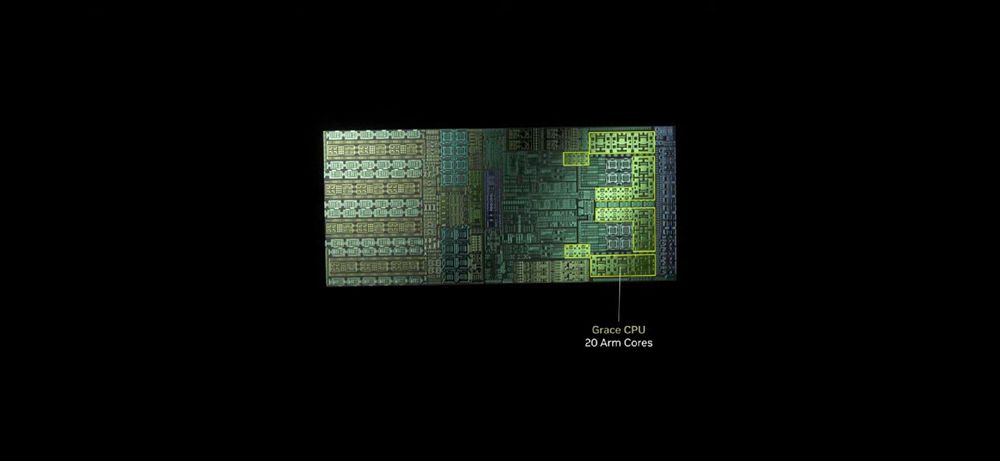
Something weird I noticed about the NVIDIA GH200 is that it's listed with 576GB of total memory, which means it isn't the expected 512GB CPU LP5X + 80GB GPU HBM3 = 592GB
GH200's memory config is actually:
-96GB GPU HBM3
-480GB CPU LP5X
/1
GH200's memory config is actually:
-96GB GPU HBM3
-480GB CPU LP5X
/1

November 23, 2024 at 1:19 PM
Something weird I noticed about the NVIDIA GH200 is that it's listed with 576GB of total memory, which means it isn't the expected 512GB CPU LP5X + 80GB GPU HBM3 = 592GB
GH200's memory config is actually:
-96GB GPU HBM3
-480GB CPU LP5X
/1
GH200's memory config is actually:
-96GB GPU HBM3
-480GB CPU LP5X
/1
All TSMC N7/N6-based Desktop GPUs plotted by Performance and Geomean of Power and Die Size, now including the RX 7600 / Navi33
This is essentially a simplified look at "Architectural Efficiency"
This is essentially a simplified look at "Architectural Efficiency"

November 23, 2024 at 1:19 PM
All TSMC N7/N6-based Desktop GPUs plotted by Performance and Geomean of Power and Die Size, now including the RX 7600 / Navi33
This is essentially a simplified look at "Architectural Efficiency"
This is essentially a simplified look at "Architectural Efficiency"
OK, it's fake
Big oops on my end
Big oops on my end

November 23, 2024 at 1:19 PM
OK, it's fake
Big oops on my end
Big oops on my end
Ryzen 7000 Series Lineup Chart

November 23, 2024 at 1:19 PM
Ryzen 7000 Series Lineup Chart
I think this flew under the radar, but Mendocino (Ryzen 7020 Series) is officially 100mm² according to AMD's website:
amd.com/en/product/121…
amd.com/en/product/121…

November 23, 2024 at 1:19 PM
I think this flew under the radar, but Mendocino (Ryzen 7020 Series) is officially 100mm² according to AMD's website:
amd.com/en/product/121…
amd.com/en/product/121…
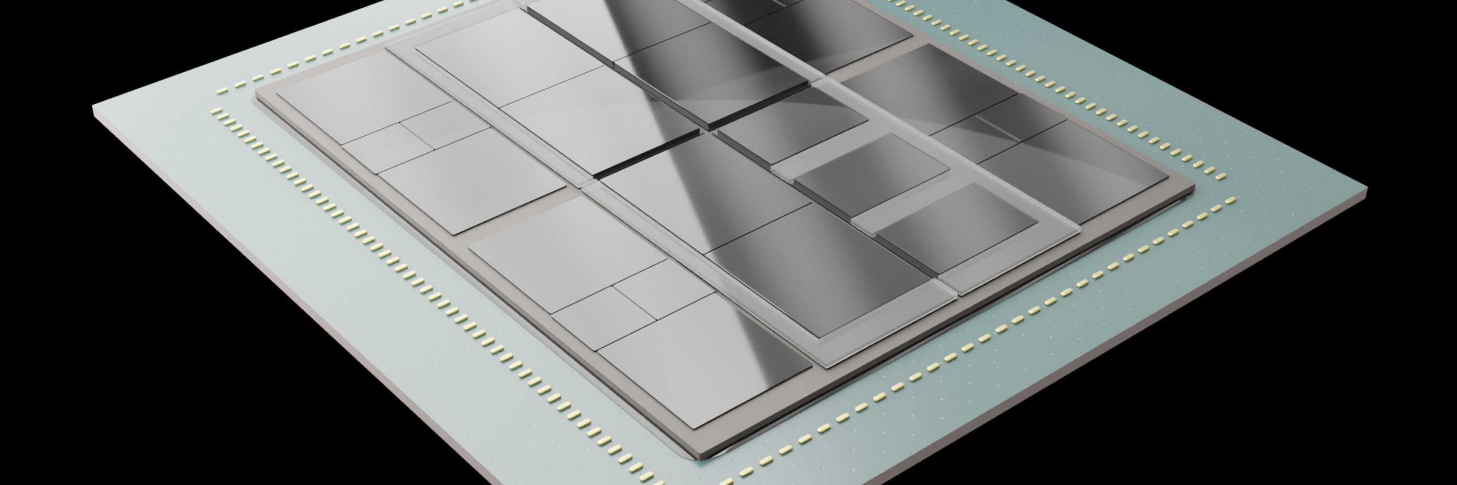
MI300 APU Renders
-4 Active Interposer Dies (AID)
-6 Accelerator Compute Dies (XCD)
-3 Core Complex Dies (CCD)
-8 Stacks of HBM3
-SH5 Socket
-3D Stacking
-Total of 146B Transistors
Everything is based on real dimensions, except for the top dies
-4 Active Interposer Dies (AID)
-6 Accelerator Compute Dies (XCD)
-3 Core Complex Dies (CCD)
-8 Stacks of HBM3
-SH5 Socket
-3D Stacking
-Total of 146B Transistors
Everything is based on real dimensions, except for the top dies

November 23, 2024 at 1:18 PM
MI300 APU Renders
-4 Active Interposer Dies (AID)
-6 Accelerator Compute Dies (XCD)
-3 Core Complex Dies (CCD)
-8 Stacks of HBM3
-SH5 Socket
-3D Stacking
-Total of 146B Transistors
Everything is based on real dimensions, except for the top dies
-4 Active Interposer Dies (AID)
-6 Accelerator Compute Dies (XCD)
-3 Core Complex Dies (CCD)
-8 Stacks of HBM3
-SH5 Socket
-3D Stacking
-Total of 146B Transistors
Everything is based on real dimensions, except for the top dies
Updated Intel Core Microarchitecture Timeline
Intel finally released Sapphire Rapids / Golden Cove-X
Intel finally released Sapphire Rapids / Golden Cove-X

November 23, 2024 at 1:18 PM
Updated Intel Core Microarchitecture Timeline
Intel finally released Sapphire Rapids / Golden Cove-X
Intel finally released Sapphire Rapids / Golden Cove-X

An overly simplistic spreadsheet of the entire Ryzen 7000 Lineup announced up to this point

November 23, 2024 at 1:18 PM
An overly simplistic spreadsheet of the entire Ryzen 7000 Lineup announced up to this point
Some notable aspects of the Ryzen 7000 mobile lineup:
-There's an R7 7736U with lower boost than the 7735U
-There's no R9 7835HS or 7040 U-Series
-R3 7335U has a 660M iGPU with 2WGPs instead of 3
-R5 7640HS has a 760M iGPU with 4WGPs instead of 3
-7040HS clocks higher than 7045HX
-There's an R7 7736U with lower boost than the 7735U
-There's no R9 7835HS or 7040 U-Series
-R3 7335U has a 660M iGPU with 2WGPs instead of 3
-R5 7640HS has a 760M iGPU with 4WGPs instead of 3
-7040HS clocks higher than 7045HX

November 23, 2024 at 1:18 PM
Some notable aspects of the Ryzen 7000 mobile lineup:
-There's an R7 7736U with lower boost than the 7735U
-There's no R9 7835HS or 7040 U-Series
-R3 7335U has a 660M iGPU with 2WGPs instead of 3
-R5 7640HS has a 760M iGPU with 4WGPs instead of 3
-7040HS clocks higher than 7045HX
-There's an R7 7736U with lower boost than the 7735U
-There's no R9 7835HS or 7040 U-Series
-R3 7335U has a 660M iGPU with 2WGPs instead of 3
-R5 7640HS has a 760M iGPU with 4WGPs instead of 3
-7040HS clocks higher than 7045HX
Wonder what node Rialto Bridge uses...
IDM 2.0 would seem to suggest it's an external foundry, so N3?
Mid-2023 would be pretty early for an HPC die on N3, even if it's ~100mm²
So maybe it's Intel 4?
Would be odd, but plausible for a more commercially viable successor to PVC
IDM 2.0 would seem to suggest it's an external foundry, so N3?
Mid-2023 would be pretty early for an HPC die on N3, even if it's ~100mm²
So maybe it's Intel 4?
Would be odd, but plausible for a more commercially viable successor to PVC

November 23, 2024 at 12:41 PM
Wonder what node Rialto Bridge uses...
IDM 2.0 would seem to suggest it's an external foundry, so N3?
Mid-2023 would be pretty early for an HPC die on N3, even if it's ~100mm²
So maybe it's Intel 4?
Would be odd, but plausible for a more commercially viable successor to PVC
IDM 2.0 would seem to suggest it's an external foundry, so N3?
Mid-2023 would be pretty early for an HPC die on N3, even if it's ~100mm²
So maybe it's Intel 4?
Would be odd, but plausible for a more commercially viable successor to PVC
If Zen4c does only cut the L3 per Core in half, then the die size of the 16C CCD would probably be ~100-110mm² when you take into account other cuts (PS5-like FPU downgrade, smaller L2, etc.)
Wonder if it could fit on the Raphael Substrate 🤔
Wonder if it could fit on the Raphael Substrate 🤔

November 23, 2024 at 12:40 PM
If Zen4c does only cut the L3 per Core in half, then the die size of the 16C CCD would probably be ~100-110mm² when you take into account other cuts (PS5-like FPU downgrade, smaller L2, etc.)
Wonder if it could fit on the Raphael Substrate 🤔
Wonder if it could fit on the Raphael Substrate 🤔
OVX Gen1 = 8x A40 + 2x ICL-SP
DGX H100 = HGX H100 (8GPU) + 2x SPR-SP
CGX = 2x(?) A16 (4GPU) + HGX Grace (2CPU)
OVX Gen2 = 4x(?) ADA? + HGX Grace (2CPU)
Maybe:
DGX GH = 4x HGX Grace Hopper ?
Would line up with what NVIDIA showed at GTC 2021
DGX H100 = HGX H100 (8GPU) + 2x SPR-SP
CGX = 2x(?) A16 (4GPU) + HGX Grace (2CPU)
OVX Gen2 = 4x(?) ADA? + HGX Grace (2CPU)
Maybe:
DGX GH = 4x HGX Grace Hopper ?
Would line up with what NVIDIA showed at GTC 2021

November 23, 2024 at 12:40 PM
OVX Gen1 = 8x A40 + 2x ICL-SP
DGX H100 = HGX H100 (8GPU) + 2x SPR-SP
CGX = 2x(?) A16 (4GPU) + HGX Grace (2CPU)
OVX Gen2 = 4x(?) ADA? + HGX Grace (2CPU)
Maybe:
DGX GH = 4x HGX Grace Hopper ?
Would line up with what NVIDIA showed at GTC 2021
DGX H100 = HGX H100 (8GPU) + 2x SPR-SP
CGX = 2x(?) A16 (4GPU) + HGX Grace (2CPU)
OVX Gen2 = 4x(?) ADA? + HGX Grace (2CPU)
Maybe:
DGX GH = 4x HGX Grace Hopper ?
Would line up with what NVIDIA showed at GTC 2021
Thinking about Zen 4's new Cache System, it would make sense if the MT Increase is higher than the ST Increase
The larger L2 would decrease L3 Hits by ~40% following the square root rule, which would decrease pressure on the Ring bus, increasing MT Perf
/1
The larger L2 would decrease L3 Hits by ~40% following the square root rule, which would decrease pressure on the Ring bus, increasing MT Perf
/1

November 23, 2024 at 12:40 PM
Thinking about Zen 4's new Cache System, it would make sense if the MT Increase is higher than the ST Increase
The larger L2 would decrease L3 Hits by ~40% following the square root rule, which would decrease pressure on the Ring bus, increasing MT Perf
/1
The larger L2 would decrease L3 Hits by ~40% following the square root rule, which would decrease pressure on the Ring bus, increasing MT Perf
/1
Does MTL-U being 2+8 mean that the tGPU is the middle die?
If so, it's definitely not on N3 (just way too big for that)
An N5-series node (or even N6) would make more sense
Wonder what they're doing with the cache system then 🤔
If so, it's definitely not on N3 (just way too big for that)
An N5-series node (or even N6) would make more sense
Wonder what they're doing with the cache system then 🤔

November 23, 2024 at 12:40 PM
Does MTL-U being 2+8 mean that the tGPU is the middle die?
If so, it's definitely not on N3 (just way too big for that)
An N5-series node (or even N6) would make more sense
Wonder what they're doing with the cache system then 🤔
If so, it's definitely not on N3 (just way too big for that)
An N5-series node (or even N6) would make more sense
Wonder what they're doing with the cache system then 🤔