


Lam Research
@lamresearch.com
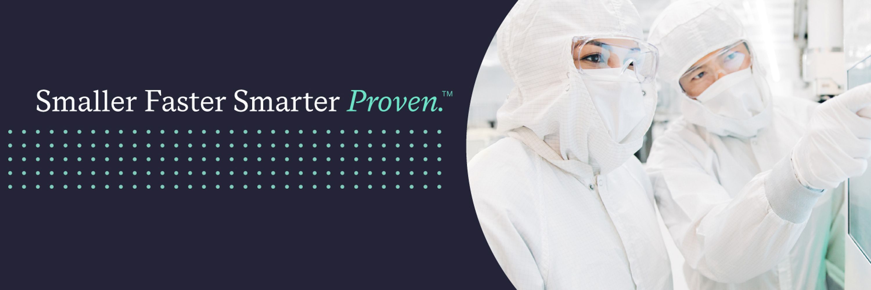
We combine superior systems engineering, technology leadership, and a commitment to customer success to advance the global semiconductor industry.
Oregon’s semiconductor ecosystem is a powerful engine for talent and ideas. From university partnerships to technical training programs, Building G strengthens our ability to engage academia and the next generation of innovators. https://bit.ly/3LPRqVj

November 21, 2025 at 9:30 PM
Oregon’s semiconductor ecosystem is a powerful engine for talent and ideas. From university partnerships to technical training programs, Building G strengthens our ability to engage academia and the next generation of innovators. https://bit.ly/3LPRqVj
Layer by layer, chipmaking magic happens. ✨ Deposition turns plasma and precision into the building blocks of advanced manufacturing, and we’ve been perfecting it for decades. Learn how via the blog. https://bit.ly/4078QSi
November 18, 2025 at 4:40 PM
Layer by layer, chipmaking magic happens. ✨ Deposition turns plasma and precision into the building blocks of advanced manufacturing, and we’ve been perfecting it for decades. Learn how via the blog. https://bit.ly/4078QSi
Akara® has entered the game. 🕹️
By leveraging DirectDrive®, a solid-state plasma source, Akara® delivers etch process control and responsiveness once thought impossible. Learn more. https://bit.ly/47I5iYK
By leveraging DirectDrive®, a solid-state plasma source, Akara® delivers etch process control and responsiveness once thought impossible. Learn more. https://bit.ly/47I5iYK
November 11, 2025 at 6:11 PM
Akara® has entered the game. 🕹️
By leveraging DirectDrive®, a solid-state plasma source, Akara® delivers etch process control and responsiveness once thought impossible. Learn more. https://bit.ly/47I5iYK
By leveraging DirectDrive®, a solid-state plasma source, Akara® delivers etch process control and responsiveness once thought impossible. Learn more. https://bit.ly/47I5iYK
The Word of the Week is void — a gap where material is missing, which can interrupt conductivity and affect overall yield. Detecting and preventing these microscopic defects helps ensure every layer performs exactly as designed.
November 5, 2025 at 8:34 PM
The Word of the Week is void — a gap where material is missing, which can interrupt conductivity and affect overall yield. Detecting and preventing these microscopic defects helps ensure every layer performs exactly as designed.
In the world of 3D chipmaking, Akara® is the real star. ⭐🎬
Here’s an inside look into CVP Gowri Kamarthy’s discussion with Counterpoint Research — out now. https://bit.ly/3Jj4D8h
Here’s an inside look into CVP Gowri Kamarthy’s discussion with Counterpoint Research — out now. https://bit.ly/3Jj4D8h
November 4, 2025 at 11:10 PM
In the world of 3D chipmaking, Akara® is the real star. ⭐🎬
Here’s an inside look into CVP Gowri Kamarthy’s discussion with Counterpoint Research — out now. https://bit.ly/3Jj4D8h
Here’s an inside look into CVP Gowri Kamarthy’s discussion with Counterpoint Research — out now. https://bit.ly/3Jj4D8h
Some masks hide identities, but ours help define them. In chipmaking, a mask protects select wafer areas during processing, guiding where intricate patterns will form before it’s lifted away.
October 29, 2025 at 3:40 PM
Some masks hide identities, but ours help define them. In chipmaking, a mask protects select wafer areas during processing, guiding where intricate patterns will form before it’s lifted away.
Dry resist, great under pressure, and built for single print patterning.
Aether® keeps things simple but never ordinary. See why it earns an “A+” in advanced nodes. https://bit.ly/47JwDuR
Aether® keeps things simple but never ordinary. See why it earns an “A+” in advanced nodes. https://bit.ly/47JwDuR
October 28, 2025 at 3:40 PM
Dry resist, great under pressure, and built for single print patterning.
Aether® keeps things simple but never ordinary. See why it earns an “A+” in advanced nodes. https://bit.ly/47JwDuR
Aether® keeps things simple but never ordinary. See why it earns an “A+” in advanced nodes. https://bit.ly/47JwDuR
3D transistor is more than a buzzword — it represents a new direction for the future of semiconductor computing. Explore how our etch and deposition solutions enable 3D transistors, including FinFET, gate-all-around, and more. https://bit.ly/4ow9dPh
October 22, 2025 at 9:45 PM
3D transistor is more than a buzzword — it represents a new direction for the future of semiconductor computing. Explore how our etch and deposition solutions enable 3D transistors, including FinFET, gate-all-around, and more. https://bit.ly/4ow9dPh
The EUV lithography process is a piece of cake with Aether® dry resist + development. 🍰
Here’s how it enables higher yield for the next generation of semiconductor devices. ⬇️ https://bit.ly/4gMXYh4
Here’s how it enables higher yield for the next generation of semiconductor devices. ⬇️ https://bit.ly/4gMXYh4
October 21, 2025 at 5:33 PM
The EUV lithography process is a piece of cake with Aether® dry resist + development. 🍰
Here’s how it enables higher yield for the next generation of semiconductor devices. ⬇️ https://bit.ly/4gMXYh4
Here’s how it enables higher yield for the next generation of semiconductor devices. ⬇️ https://bit.ly/4gMXYh4
See how we use virtual twins to catch etch loading effects that impact uniformity and yield, faster and at a lower cost than traditional testing. https://bit.ly/3KTuHHn

October 17, 2025 at 7:21 PM
See how we use virtual twins to catch etch loading effects that impact uniformity and yield, faster and at a lower cost than traditional testing. https://bit.ly/3KTuHHn
Revisiting Lam milestones from the past. 🪣⛏️
See what’s in our 1988 time capsule.
See what’s in our 1988 time capsule.
October 16, 2025 at 4:10 PM
Revisiting Lam milestones from the past. 🪣⛏️
See what’s in our 1988 time capsule.
See what’s in our 1988 time capsule.
Our contributions to the Colorado School of Mines earned us the Mines@150 Visionary award! See how we support semiconductor research in higher education via the blog. https://bit.ly/3JdcWlN


October 14, 2025 at 7:32 PM
Our contributions to the Colorado School of Mines earned us the Mines@150 Visionary award! See how we support semiconductor research in higher education via the blog. https://bit.ly/3JdcWlN
When chips get complex, Akara® gets precise. Shrinking architectures and rising performance demands don’t leave much room for error — but that’s exactly where our newest conductor etch system, Akara®, shines. ✨ Tap the link to explore. bit.ly/4i5iURo
October 14, 2025 at 5:20 PM
When chips get complex, Akara® gets precise. Shrinking architectures and rising performance demands don’t leave much room for error — but that’s exactly where our newest conductor etch system, Akara®, shines. ✨ Tap the link to explore. bit.ly/4i5iURo
Hot off the press from SEMICON West: Lam Cryo ™ 3.0 earned us the 2025 SEMI Award. 🏆🎉 Check it out. https://bit.ly/48spTm9

October 9, 2025 at 5:31 PM
Hot off the press from SEMICON West: Lam Cryo ™ 3.0 earned us the 2025 SEMI Award. 🏆🎉 Check it out. https://bit.ly/48spTm9
Ready for another Word of the Week?
Today’s word is capacitor, a component that stores an electric charge in logic and memory chips, consisting of conductors separated by an insulator.⚡ https://bit.ly/4nGxfaa
Today’s word is capacitor, a component that stores an electric charge in logic and memory chips, consisting of conductors separated by an insulator.⚡ https://bit.ly/4nGxfaa
October 8, 2025 at 7:31 PM
Ready for another Word of the Week?
Today’s word is capacitor, a component that stores an electric charge in logic and memory chips, consisting of conductors separated by an insulator.⚡ https://bit.ly/4nGxfaa
Today’s word is capacitor, a component that stores an electric charge in logic and memory chips, consisting of conductors separated by an insulator.⚡ https://bit.ly/4nGxfaa
Time is everything in semiconductor manufacturing. Fabtex™ Yield Optimizer reshapes the path to high yields by combining AI, machine learning, and digital twins with real fab data. The result: fewer iterations, faster ramp, and reduced scrap. Discover more. https://bit.ly/47bVMxX

October 7, 2025 at 3:00 PM
Time is everything in semiconductor manufacturing. Fabtex™ Yield Optimizer reshapes the path to high yields by combining AI, machine learning, and digital twins with real fab data. The result: fewer iterations, faster ramp, and reduced scrap. Discover more. https://bit.ly/47bVMxX
Building on decades of dielectric film and advanced packaging solutions, we introduced our most advanced deposition tool to date.
Learn how VECTOR® TEOS 3D delivers high-quality, void-free thick dielectric film deposition for advanced packaging.
Learn how VECTOR® TEOS 3D delivers high-quality, void-free thick dielectric film deposition for advanced packaging.
October 2, 2025 at 5:36 PM
Building on decades of dielectric film and advanced packaging solutions, we introduced our most advanced deposition tool to date.
Learn how VECTOR® TEOS 3D delivers high-quality, void-free thick dielectric film deposition for advanced packaging.
Learn how VECTOR® TEOS 3D delivers high-quality, void-free thick dielectric film deposition for advanced packaging.
Plasma etch is like a sculptor’s tool at the atomic level. See how our etch systems shape nanoscale features with precision. ➡️ https://bit.ly/4mji5qd
October 1, 2025 at 5:00 PM
Plasma etch is like a sculptor’s tool at the atomic level. See how our etch systems shape nanoscale features with precision. ➡️ https://bit.ly/4mji5qd
Where AI’s demand for massive computing creates challenges, advanced packaging offers a solution.
Discover how advanced packaging enables the creation of powerful AI chips while optimizing performance, cost, and more. https://bit.ly/42GBLwW
Discover how advanced packaging enables the creation of powerful AI chips while optimizing performance, cost, and more. https://bit.ly/42GBLwW
September 29, 2025 at 4:00 PM
Where AI’s demand for massive computing creates challenges, advanced packaging offers a solution.
Discover how advanced packaging enables the creation of powerful AI chips while optimizing performance, cost, and more. https://bit.ly/42GBLwW
Discover how advanced packaging enables the creation of powerful AI chips while optimizing performance, cost, and more. https://bit.ly/42GBLwW
Enter the advanced packaging era. Watch our advanced packaging tools solve etch, bond, and deposition challenges layer by layer, die by die.
September 25, 2025 at 5:01 PM
Enter the advanced packaging era. Watch our advanced packaging tools solve etch, bond, and deposition challenges layer by layer, die by die.
A redistribution layer is like GPS on a wafer, allowing chipmakers to re-route conductive points during the packaging process and improve overall chip performance! 🛣️🚗
Our SABRE® 3D products use this extra metal layer — learn more. https://bit.ly/46T6old
Our SABRE® 3D products use this extra metal layer — learn more. https://bit.ly/46T6old
September 24, 2025 at 5:00 PM
A redistribution layer is like GPS on a wafer, allowing chipmakers to re-route conductive points during the packaging process and improve overall chip performance! 🛣️🚗
Our SABRE® 3D products use this extra metal layer — learn more. https://bit.ly/46T6old
Our SABRE® 3D products use this extra metal layer — learn more. https://bit.ly/46T6old
Leveraging our deep expertise in atomic layer deposition (ALD), we created ALTUS® Halo. See how our next generation ALD tool enables a new era of semiconductor metallization with the adoption of molybdenum. bit.ly/4mrZg3N
September 23, 2025 at 4:56 PM
Leveraging our deep expertise in atomic layer deposition (ALD), we created ALTUS® Halo. See how our next generation ALD tool enables a new era of semiconductor metallization with the adoption of molybdenum. bit.ly/4mrZg3N
High bandwidth memory (HBM) stacks layers and scales efficiently, moving data at massive bandwidths to power AI computing. See how we play a key role via our blog. https://bit.ly/3Vq7Kxq

September 19, 2025 at 5:30 PM
High bandwidth memory (HBM) stacks layers and scales efficiently, moving data at massive bandwidths to power AI computing. See how we play a key role via our blog. https://bit.ly/3Vq7Kxq
Advanced packaging is the hidden engine behind every AI advancement. This technology powers faster performance and greater efficiency.
Learn how via our blog. https://bit.ly/3VlbYqa
Learn how via our blog. https://bit.ly/3VlbYqa

September 18, 2025 at 10:48 PM
Advanced packaging is the hidden engine behind every AI advancement. This technology powers faster performance and greater efficiency.
Learn how via our blog. https://bit.ly/3VlbYqa
Learn how via our blog. https://bit.ly/3VlbYqa
Did you know ALTUS® Halo deposits barrier-free molybdenum with greater than 50% reduction in word line resistance over tungsten?
Leading high-volume manufacturers of 3D NAND have already transitioned to molybdenum — learn why from Counterpoint Research. https://bit.ly/3JYUVb5
Leading high-volume manufacturers of 3D NAND have already transitioned to molybdenum — learn why from Counterpoint Research. https://bit.ly/3JYUVb5
September 16, 2025 at 7:03 PM
Did you know ALTUS® Halo deposits barrier-free molybdenum with greater than 50% reduction in word line resistance over tungsten?
Leading high-volume manufacturers of 3D NAND have already transitioned to molybdenum — learn why from Counterpoint Research. https://bit.ly/3JYUVb5
Leading high-volume manufacturers of 3D NAND have already transitioned to molybdenum — learn why from Counterpoint Research. https://bit.ly/3JYUVb5