


Jonas Sundqvist
@jv3sund.bsky.social
CEO AlixLabs and BALD Engineering
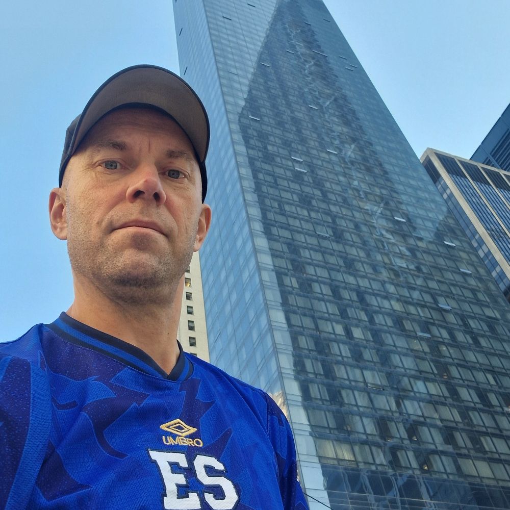
The conference hotel has two drinks announced for tonight as drink of the month - is this the same cocktail? @seanbarry.bsky.social


October 29, 2025 at 1:34 PM
The conference hotel has two drinks announced for tonight as drink of the month - is this the same cocktail? @seanbarry.bsky.social
Valhalla has arrived from across the pond - stay tuned for more information. Ymir is ready to open the first gate valve to fully automated 300 mm APS(TM) processing for our customers. #AlixLabs #Sweden #Semiconductor #ALEtch

October 22, 2025 at 8:58 PM
Valhalla has arrived from across the pond - stay tuned for more information. Ymir is ready to open the first gate valve to fully automated 300 mm APS(TM) processing for our customers. #AlixLabs #Sweden #Semiconductor #ALEtch

September 21, 2025 at 7:59 PM

September 11, 2025 at 5:55 AM
Have a nice weekend @mick--geek.bsky.social

June 27, 2025 at 5:09 PM
Have a nice weekend @mick--geek.bsky.social
Henrik used the ring @drhenke.bsky.social #aldep

June 25, 2025 at 6:11 AM
Henrik used the ring @drhenke.bsky.social #aldep


Remember that literally armies of one half cycle precursor nozxles for hydrogen peroxide metal oxide #ALDep roams freely in nature. In an coordinated attack these ants could print a high-k device if there were TMA ants.

May 23, 2025 at 4:03 AM
Remember that literally armies of one half cycle precursor nozxles for hydrogen peroxide metal oxide #ALDep roams freely in nature. In an coordinated attack these ants could print a high-k device if there were TMA ants.


May 6, 2025 at 2:03 PM
Congratulations 🎊
@mick--geek.bsky.social
@mick--geek.bsky.social

May 4, 2025 at 6:23 PM
Congratulations 🎊
@mick--geek.bsky.social
@mick--geek.bsky.social
Yes also the Swedish version

April 12, 2025 at 1:34 PM
Yes also the Swedish version
Hobitti - I did not know @rlpuu.bsky.social


April 11, 2025 at 7:05 PM
Hobitti - I did not know @rlpuu.bsky.social

April 11, 2025 at 5:40 AM
🎤 AlixLabs on Stage at the SOLD OUT 2025 CMC Conference!
🕓 4:00 PM | March 29 | Bergström Ballroom
👨🔬 Dr. Robin Athle, Principal Engineer
"Atomic Layer Etching Pitch Splitting (APS): A New Alternative to Multi Patterning"
#ALEtch #Semiconductors #Lithography #Texas #USA #Austin
🕓 4:00 PM | March 29 | Bergström Ballroom
👨🔬 Dr. Robin Athle, Principal Engineer
"Atomic Layer Etching Pitch Splitting (APS): A New Alternative to Multi Patterning"
#ALEtch #Semiconductors #Lithography #Texas #USA #Austin

March 29, 2025 at 7:04 AM
🎤 AlixLabs on Stage at the SOLD OUT 2025 CMC Conference!
🕓 4:00 PM | March 29 | Bergström Ballroom
👨🔬 Dr. Robin Athle, Principal Engineer
"Atomic Layer Etching Pitch Splitting (APS): A New Alternative to Multi Patterning"
#ALEtch #Semiconductors #Lithography #Texas #USA #Austin
🕓 4:00 PM | March 29 | Bergström Ballroom
👨🔬 Dr. Robin Athle, Principal Engineer
"Atomic Layer Etching Pitch Splitting (APS): A New Alternative to Multi Patterning"
#ALEtch #Semiconductors #Lithography #Texas #USA #Austin
Today vi visit Odins possible birth place @alixlabs.bsky.social

March 26, 2025 at 6:33 AM
Today vi visit Odins possible birth place @alixlabs.bsky.social
@mick--geek.bsky.social Facebook algorithm after meeting you and praising your Judas t-shirt

March 25, 2025 at 6:55 PM
@mick--geek.bsky.social Facebook algorithm after meeting you and praising your Judas t-shirt
Probably the best poster at #ASD2025 in Leipzig. Talk to us if you need help with the analysis @alixlabs.bsky.social!

March 25, 2025 at 4:11 PM
Probably the best poster at #ASD2025 in Leipzig. Talk to us if you need help with the analysis @alixlabs.bsky.social!


March 23, 2025 at 12:09 PM
Chipmetrics launches the PillarHall LHAR5 test chip, featuring a 100-nm gap height for precise process monitoring. It enables vendor-agnostic benchmarking, faster tool qual, & sustainable manufacturing, ensuring tighter control for 3DNAND & 3DDRAM advancements. #ALDep chipmetrics.com/the-pillarha...

February 10, 2025 at 8:05 PM
Chipmetrics launches the PillarHall LHAR5 test chip, featuring a 100-nm gap height for precise process monitoring. It enables vendor-agnostic benchmarking, faster tool qual, & sustainable manufacturing, ensuring tighter control for 3DNAND & 3DDRAM advancements. #ALDep chipmetrics.com/the-pillarha...
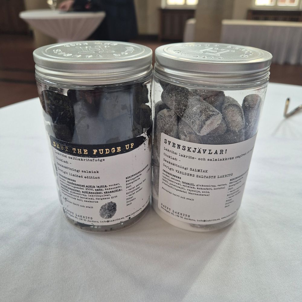
Reeespect! Our Norwegian exchange student left us some Lakrits! Did I tell you I love Norway 🇳🇴?

February 7, 2025 at 7:53 PM
Reeespect! Our Norwegian exchange student left us some Lakrits! Did I tell you I love Norway 🇳🇴?
AlixLabs to Showcase Latest APS™ Findings at SPIE Advanced Lithography + Patterning
Swedish semiconductor startup to demonstrate 3-nanometer class FinFET structures made with APS™ on Intel Silicon at trade show. @alixlabs.bsky.social #ALEtch #Semiconductor
www.alixlabs.com/2025/02/07/a...
Swedish semiconductor startup to demonstrate 3-nanometer class FinFET structures made with APS™ on Intel Silicon at trade show. @alixlabs.bsky.social #ALEtch #Semiconductor
www.alixlabs.com/2025/02/07/a...

February 7, 2025 at 7:18 AM
AlixLabs to Showcase Latest APS™ Findings at SPIE Advanced Lithography + Patterning
Swedish semiconductor startup to demonstrate 3-nanometer class FinFET structures made with APS™ on Intel Silicon at trade show. @alixlabs.bsky.social #ALEtch #Semiconductor
www.alixlabs.com/2025/02/07/a...
Swedish semiconductor startup to demonstrate 3-nanometer class FinFET structures made with APS™ on Intel Silicon at trade show. @alixlabs.bsky.social #ALEtch #Semiconductor
www.alixlabs.com/2025/02/07/a...
Coming 2025 - APS(TM) 300mm Platform. AlixLabs Introduces 300mm APS™ to Enable Small Nodes at Low Cost. #semiconductor @alixlabs.bsky.social #TeamSweden #Sweden #APSTM #ALEtch


February 6, 2025 at 6:20 AM
Coming 2025 - APS(TM) 300mm Platform. AlixLabs Introduces 300mm APS™ to Enable Small Nodes at Low Cost. #semiconductor @alixlabs.bsky.social #TeamSweden #Sweden #APSTM #ALEtch
Ett forskningssamarbete kring galliumnitrid (GaN) och indiumnitrid (InN) inleds nu mellan Alixlabs i Lund Pedersengruppen på Linköpings universitet. etn.se/index.php/ny... @alixlabs.bsky.social @drhenke.bsky.social @liu.se

February 6, 2025 at 6:18 AM
Ett forskningssamarbete kring galliumnitrid (GaN) och indiumnitrid (InN) inleds nu mellan Alixlabs i Lund Pedersengruppen på Linköpings universitet. etn.se/index.php/ny... @alixlabs.bsky.social @drhenke.bsky.social @liu.se
ALD/ALE 2025 Submission # 10785 by
@alixlabs.bsky.social
We will be showing off the smallest high aspect ratio fin that we´ve done, 19 atoms across. Amongst other things!
Abstract submission closes Thursday, February 6, 2025 4:59 AM UTC. #Korea #ALDep #ALEtch #Semiconductor #ALDALE2025
@alixlabs.bsky.social
We will be showing off the smallest high aspect ratio fin that we´ve done, 19 atoms across. Amongst other things!
Abstract submission closes Thursday, February 6, 2025 4:59 AM UTC. #Korea #ALDep #ALEtch #Semiconductor #ALDALE2025


February 4, 2025 at 9:44 PM
ALD/ALE 2025 Submission # 10785 by
@alixlabs.bsky.social
We will be showing off the smallest high aspect ratio fin that we´ve done, 19 atoms across. Amongst other things!
Abstract submission closes Thursday, February 6, 2025 4:59 AM UTC. #Korea #ALDep #ALEtch #Semiconductor #ALDALE2025
@alixlabs.bsky.social
We will be showing off the smallest high aspect ratio fin that we´ve done, 19 atoms across. Amongst other things!
Abstract submission closes Thursday, February 6, 2025 4:59 AM UTC. #Korea #ALDep #ALEtch #Semiconductor #ALDALE2025