
Han-Bo-Ram (Boram) Lee
@hbrlee.bsky.social
Professor of MSE, Incheon National University
Associate Editor of Chemistry of Materials, American Chemical Society
Associate Editor of Chemistry of Materials, American Chemical Society
I’ll be speaking at the Thin Film Society webinar on Dec 17!
“Atomic Layer Innovations: New Pathways for Future Semiconductor Fabrication”
• #ASDep for future patterning
• AI-driven materials design via #ALDep
🕘 9 PM Seoul / 1 PM CET / 7 AM EST
🔗 voovmeeting.com/dm/xrmEzmbmY...
“Atomic Layer Innovations: New Pathways for Future Semiconductor Fabrication”
• #ASDep for future patterning
• AI-driven materials design via #ALDep
🕘 9 PM Seoul / 1 PM CET / 7 AM EST
🔗 voovmeeting.com/dm/xrmEzmbmY...

December 6, 2025 at 2:02 AM
I’ll be speaking at the Thin Film Society webinar on Dec 17!
“Atomic Layer Innovations: New Pathways for Future Semiconductor Fabrication”
• #ASDep for future patterning
• AI-driven materials design via #ALDep
🕘 9 PM Seoul / 1 PM CET / 7 AM EST
🔗 voovmeeting.com/dm/xrmEzmbmY...
“Atomic Layer Innovations: New Pathways for Future Semiconductor Fabrication”
• #ASDep for future patterning
• AI-driven materials design via #ALDep
🕘 9 PM Seoul / 1 PM CET / 7 AM EST
🔗 voovmeeting.com/dm/xrmEzmbmY...
Our new paper in Applied Surface Science explores #ASDep of W and Ru using a Homometallic Precursor Inhibitor approach.
Yes—we actively look for bad #ALDep precursors as inhibitors!
Free to read/download until Jan 4th. authors.elsevier.com/a/1m6NhcXa-C...
Yes—we actively look for bad #ALDep precursors as inhibitors!
Free to read/download until Jan 4th. authors.elsevier.com/a/1m6NhcXa-C...
authors.elsevier.com
November 15, 2025 at 7:11 AM
Our new paper in Applied Surface Science explores #ASDep of W and Ru using a Homometallic Precursor Inhibitor approach.
Yes—we actively look for bad #ALDep precursors as inhibitors!
Free to read/download until Jan 4th. authors.elsevier.com/a/1m6NhcXa-C...
Yes—we actively look for bad #ALDep precursors as inhibitors!
Free to read/download until Jan 4th. authors.elsevier.com/a/1m6NhcXa-C...
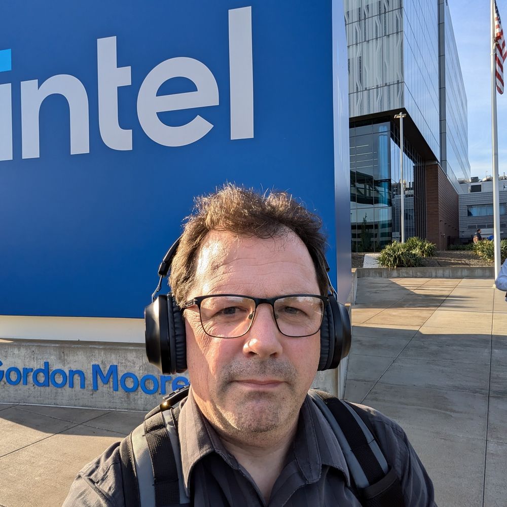
I gave a seminar on the silicon chip industry and the importance of device fabrication at Incheon POSCO High School (인천포스코 고등학교). It’s always a great joy to meet highly motivated young students.


May 15, 2025 at 1:14 AM
I gave a seminar on the silicon chip industry and the importance of device fabrication at Incheon POSCO High School (인천포스코 고등학교). It’s always a great joy to meet highly motivated young students.


As you know, patterning technology has not traditionally played a central role.
However, things have changed. Achieving nanoscale patterns with high reliability is now extremely challenging, and patterning is no longer just a supporting technique.
pubs.acs.org/page/cmatex/...
However, things have changed. Achieving nanoscale patterns with high reliability is now extremely challenging, and patterning is no longer just a supporting technique.
pubs.acs.org/page/cmatex/...
Precision Patterning
pubs.acs.org
April 2, 2025 at 12:02 AM
As you know, patterning technology has not traditionally played a central role.
However, things have changed. Achieving nanoscale patterns with high reliability is now extremely challenging, and patterning is no longer just a supporting technique.
pubs.acs.org/page/cmatex/...
However, things have changed. Achieving nanoscale patterns with high reliability is now extremely challenging, and patterning is no longer just a supporting technique.
pubs.acs.org/page/cmatex/...
Reposted by Han-Bo-Ram (Boram) Lee
This is a great community of chemists, physicists and engineers, academics and industry. Love it! #ASD2025 @asd2025leipzig.bsky.social
March 23, 2025 at 7:42 PM
This is a great community of chemists, physicists and engineers, academics and industry. Love it! #ASD2025 @asd2025leipzig.bsky.social
Reposted by Han-Bo-Ram (Boram) Lee
@cathleencrudden.bsky.social presenting the third tutorial at #ASD2025 introducing us to how crazy is it that ligands impart totally different properties to a metal.
Also warning us to avoid Ni(CO)4
Also warning us to avoid Ni(CO)4

March 23, 2025 at 3:42 PM
@cathleencrudden.bsky.social presenting the third tutorial at #ASD2025 introducing us to how crazy is it that ligands impart totally different properties to a metal.
Also warning us to avoid Ni(CO)4
Also warning us to avoid Ni(CO)4
Group holiday season party!


December 13, 2024 at 3:57 AM
Group holiday season party!