


Peter Goossens
@goossens66peter.bsky.social
RF prototyping, design and test equipment. Creator of Gquipment.
www.gquipment.com
www.gquipment.com
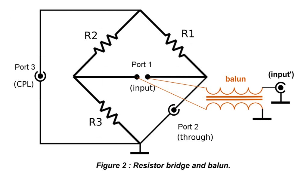
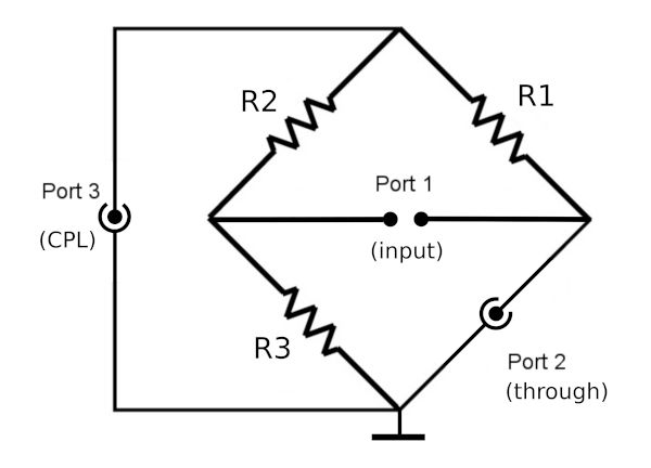
In practice, resistor bridge couplers face several challenges. The first challenge arises because the input port (port 1) is balanced. Therefore a balun is required. It sets a lower frequency limit and, more problematically, can disturb the bridge balance because it operates in parallel with R3.
January 29, 2025 at 12:54 PM
In practice, resistor bridge couplers face several challenges. The first challenge arises because the input port (port 1) is balanced. Therefore a balun is required. It sets a lower frequency limit and, more problematically, can disturb the bridge balance because it operates in parallel with R3.
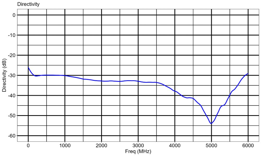
Now, the question arises: how can such a device be designed to achieve good directivity over a wide frequency span? The solution is to use a balanced resistor bridge. Because it relies on resistors, this design achieves a bandwidth starting at DC and extending easily into double-digit GHz.
January 29, 2025 at 12:54 PM
Now, the question arises: how can such a device be designed to achieve good directivity over a wide frequency span? The solution is to use a balanced resistor bridge. Because it relies on resistors, this design achieves a bandwidth starting at DC and extending easily into double-digit GHz.
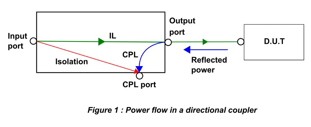
These couplers are used to measure incident or reflected power. They are utilized in VNAs, antenna analyzers, and laboratory settings to measure output power or impedance mismatch using a spectrum analyzer. Figure 1 illustrates the power flow when a coupler is used to measure reflected power.
January 29, 2025 at 12:54 PM
These couplers are used to measure incident or reflected power. They are utilized in VNAs, antenna analyzers, and laboratory settings to measure output power or impedance mismatch using a spectrum analyzer. Figure 1 illustrates the power flow when a coupler is used to measure reflected power.
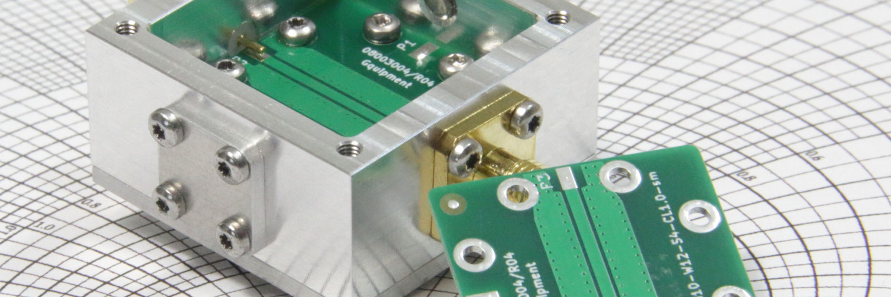
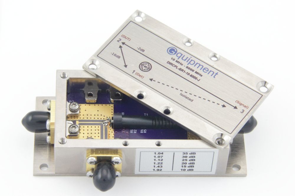
What's inside a wideband directional coupler? The lid of the box lifted. A thread🧵..
#RFDesign #KiCad #RFEngineering #gquipment
#RFDesign #KiCad #RFEngineering #gquipment
January 29, 2025 at 12:54 PM
What's inside a wideband directional coupler? The lid of the box lifted. A thread🧵..
#RFDesign #KiCad #RFEngineering #gquipment
#RFDesign #KiCad #RFEngineering #gquipment
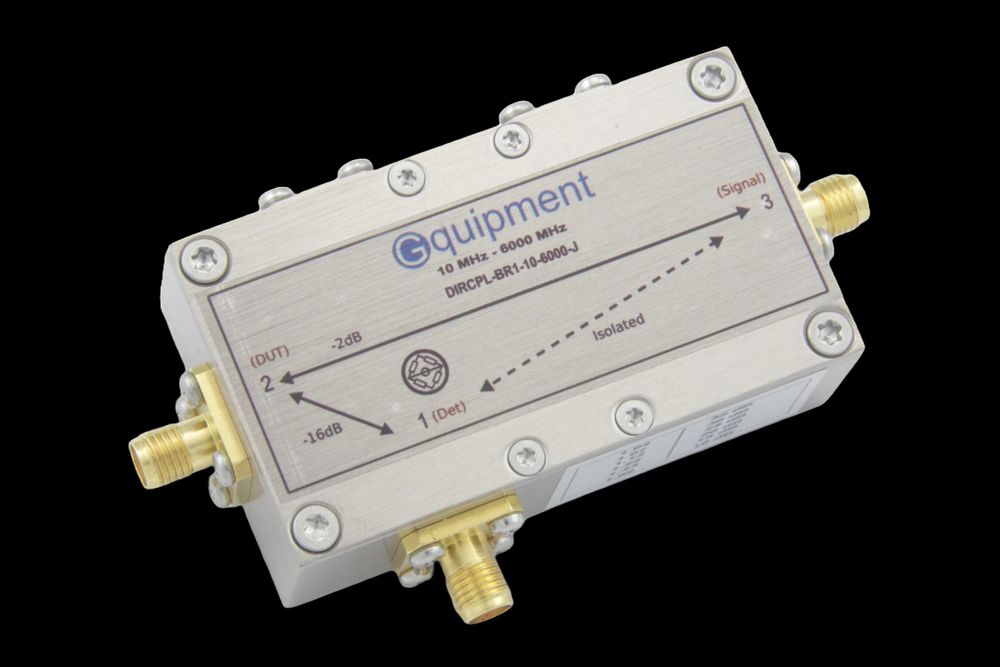
New: Introducing a 10 MHz - 6000 MHz wide band directional coupler (DIRCPL-BR1-16-10-6000). You can find it in the web shop.
Specs: 2 dB insertion loss, 16 dB coupling, -30 dB directivity, 10 - 6000 MHz
www.gquipment.com/28-rf-direct...
#RFDesign #PCB #KiCad
Specs: 2 dB insertion loss, 16 dB coupling, -30 dB directivity, 10 - 6000 MHz
www.gquipment.com/28-rf-direct...
#RFDesign #PCB #KiCad
January 14, 2025 at 9:54 AM
New: Introducing a 10 MHz - 6000 MHz wide band directional coupler (DIRCPL-BR1-16-10-6000). You can find it in the web shop.
Specs: 2 dB insertion loss, 16 dB coupling, -30 dB directivity, 10 - 6000 MHz
www.gquipment.com/28-rf-direct...
#RFDesign #PCB #KiCad
Specs: 2 dB insertion loss, 16 dB coupling, -30 dB directivity, 10 - 6000 MHz
www.gquipment.com/28-rf-direct...
#RFDesign #PCB #KiCad
January 13, 2025 at 8:08 AM
8/8 The two images illustrate the results for the generated spectrum at Fout = 50 MHz and Fout = 50.0045 MHz. Both outputs were generated using the fractional algorithm. As you can see, just a small change in Fout can lead to a significant increase in spurs.


December 4, 2024 at 12:38 PM
8/8 The two images illustrate the results for the generated spectrum at Fout = 50 MHz and Fout = 50.0045 MHz. Both outputs were generated using the fractional algorithm. As you can see, just a small change in Fout can lead to a significant increase in spurs.
7/8 A test setup was created using standard development boards for the Si5351A PLL and the ST32MCU. The MCU controls the PLL parameters by sending them via I2C.

December 4, 2024 at 12:38 PM
7/8 A test setup was created using standard development boards for the Si5351A PLL and the ST32MCU. The MCU controls the PLL parameters by sending them via I2C.
6/8 The fractional algorithm uses a fractional value for N, expressed as A+B/C. The GCD is used to compute B/C, ensuring C is the smallest possible denominator. This approach provides an exact solution. However, if C exceeds the PLL’s supported range, it is capped, which sacrifices precision.

December 4, 2024 at 12:38 PM
6/8 The fractional algorithm uses a fractional value for N, expressed as A+B/C. The GCD is used to compute B/C, ensuring C is the smallest possible denominator. This approach provides an exact solution. However, if C exceeds the PLL’s supported range, it is capped, which sacrifices precision.
5/8 The integer-only algorithm employs the Least Common Multiple (LCM) of Fref and Fout to determine Fvco. The LCM is calculated using the Greatest Common Divisor (GCD).

December 4, 2024 at 12:38 PM
5/8 The integer-only algorithm employs the Least Common Multiple (LCM) of Fref and Fout to determine Fvco. The LCM is calculated using the Greatest Common Divisor (GCD).
3/8 To make a PLL generate a required Fout, you must determine the appropriate values for Fref, N, and D. Additionally, a real-life PLL has a limited range for Fvco, which serves as a boundary condition. Often, Fref is a fixed value.

December 4, 2024 at 12:38 PM
3/8 To make a PLL generate a required Fout, you must determine the appropriate values for Fref, N, and D. Additionally, a real-life PLL has a limited range for Fvco, which serves as a boundary condition. Often, Fref is a fixed value.
2/8 In general, a PLL uses a reference frequency (Fref), has a VCO that operates at Fvco, and employs a feedback divisor N and an output divisor D. The combination of these variables ensures the PLL generates a specific output frequency (Fout).

December 4, 2024 at 12:38 PM
2/8 In general, a PLL uses a reference frequency (Fref), has a VCO that operates at Fvco, and employs a feedback divisor N and an output divisor D. The combination of these variables ensures the PLL generates a specific output frequency (Fout).
1/8 How to configure a PLL synthesizer using algorithms that find exact solutions? Here’s a demonstration with the Si5351A PLL.
#gquipment #PLL #RFDesign
#gquipment #PLL #RFDesign

December 4, 2024 at 12:38 PM
1/8 How to configure a PLL synthesizer using algorithms that find exact solutions? Here’s a demonstration with the Si5351A PLL.
#gquipment #PLL #RFDesign
#gquipment #PLL #RFDesign
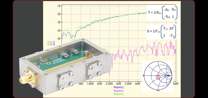
6/7. Next I measured a 50 ohm termination resistor using the same RF-MINI-ENCL as fixture. This time, I tried to make a more accurate model of the fixture. The images show the measurement data (without de-embedding).


November 26, 2024 at 1:04 PM
6/7. Next I measured a 50 ohm termination resistor using the same RF-MINI-ENCL as fixture. This time, I tried to make a more accurate model of the fixture. The images show the measurement data (without de-embedding).
5/7. The de-embedded plots of insertion loss, return loss, and impedance illustrate that below 5 GHz, all parameters are closer to their expected values. The effect is most noticeable in the impedance plot. De-embedding has eliminated the phase change effect of the fixture.


November 26, 2024 at 1:04 PM
5/7. The de-embedded plots of insertion loss, return loss, and impedance illustrate that below 5 GHz, all parameters are closer to their expected values. The effect is most noticeable in the impedance plot. De-embedding has eliminated the phase change effect of the fixture.
3/7. To eliminate the effects of the fixture, one must somehow now the S-parameters of the fixture. I derived them by modeling the fixture and utilizing a simulator (Qucs) to obtain its S-parameters.

November 26, 2024 at 1:04 PM
3/7. To eliminate the effects of the fixture, one must somehow now the S-parameters of the fixture. I derived them by modeling the fixture and utilizing a simulator (Qucs) to obtain its S-parameters.
2/7. I started by measuring the S-parameters of a 100 ohm resistor. With a 100 ohm resistor, reflection and insertion loss are both -6 dB. I used an RF-ENCL-MINI as a test fixture. The pictures show the measured insertion and return loss and also an impedance plot.


November 26, 2024 at 1:04 PM
2/7. I started by measuring the S-parameters of a 100 ohm resistor. With a 100 ohm resistor, reflection and insertion loss are both -6 dB. I used an RF-ENCL-MINI as a test fixture. The pictures show the measured insertion and return loss and also an impedance plot.
1/7. I did some experiments to de-embedding S-parameters to remove the effects of a test fixture using a Octave/Matlab script processing the raw measurement data. This script uses T-parameters to remove the effects of the fixture.
November 26, 2024 at 1:04 PM
1/7. I did some experiments to de-embedding S-parameters to remove the effects of a test fixture using a Octave/Matlab script processing the raw measurement data. This script uses T-parameters to remove the effects of the fixture.
Spurious frequencies. STM32 is controlling a Si5351A PLL in integer mode. Signal is split and watched on an oscilloscope and a spectrum analyser. Look at the differences in spurious frequencies at each step.
November 23, 2024 at 10:59 AM
Spurious frequencies. STM32 is controlling a Si5351A PLL in integer mode. Signal is split and watched on an oscilloscope and a spectrum analyser. Look at the differences in spurious frequencies at each step.
Directional bridge. Above 3 GHz and for directivity < -30 dB, everything matters: position and orientation of resistors, all parasitics, PCB layout, impedance of outer shield (also acting as a transmission line), resonances along that line, and matching of SMA connectors. Your job: balance them all.


November 23, 2024 at 10:02 AM
Directional bridge. Above 3 GHz and for directivity < -30 dB, everything matters: position and orientation of resistors, all parasitics, PCB layout, impedance of outer shield (also acting as a transmission line), resonances along that line, and matching of SMA connectors. Your job: balance them all.
2/3. Example of PCB 08003017
FR4, 26.8 x 26.8 mm, 1.0 mm substrate thickness.
FR4, 26.8 x 26.8 mm, 1.0 mm substrate thickness.


November 22, 2024 at 10:47 AM
2/3. Example of PCB 08003017
FR4, 26.8 x 26.8 mm, 1.0 mm substrate thickness.
FR4, 26.8 x 26.8 mm, 1.0 mm substrate thickness.
1/3. Created several example PCBs. They all show different solutions for implementing a transmission line with a combination of RF Enclosure Mini, SMA connector type and tline configuration.
#gquipment #RFDesign #KiCad
#gquipment #RFDesign #KiCad

November 22, 2024 at 10:47 AM
1/3. Created several example PCBs. They all show different solutions for implementing a transmission line with a combination of RF Enclosure Mini, SMA connector type and tline configuration.
#gquipment #RFDesign #KiCad
#gquipment #RFDesign #KiCad
Over the next few days I'll be copying some messages from Twitter (X) here. I hope you don't get too bored with content you may have seen before.

November 21, 2024 at 3:22 PM
Over the next few days I'll be copying some messages from Twitter (X) here. I hope you don't get too bored with content you may have seen before.
Web based tool to read S-parameter files and produce a plot file (actually, a PNG). It is a spin-off of my effort to simplify the process of making good looking images after doing some VNA measurements.
gquipment.shinyapps.io/S-Parameter-...
#Sparameters #VNA
gquipment.shinyapps.io/S-Parameter-...
#Sparameters #VNA

November 21, 2024 at 3:18 PM
Web based tool to read S-parameter files and produce a plot file (actually, a PNG). It is a spin-off of my effort to simplify the process of making good looking images after doing some VNA measurements.
gquipment.shinyapps.io/S-Parameter-...
#Sparameters #VNA
gquipment.shinyapps.io/S-Parameter-...
#Sparameters #VNA

November 20, 2024 at 12:59 PM